


Now Reading: Breakthrough Brings 2D Transistors Closer to Reality
-
01
Breakthrough Brings 2D Transistors Closer to Reality
Speedy Summary
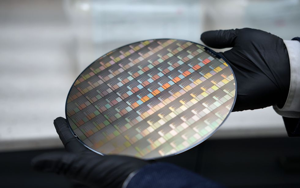
- Chipmaking giants like Intel, Samsung, and TSMC are advancing efforts to use 2D semiconductors (like molybdenum disulfide) in transistors-a move initially projected to be more than a decade away.
- MIT-spun startup CDimension claims it has achieved a low-temperature process (200 °C) for growing MoS₂ directly on silicon wafers without damaging existing circuits.
- This breakthrough enables multitiered 3D chip architectures by integrating layers of 2D transistors above existing silicon circuits, addressing wafer-scale uniformity and reliability concerns.
- CDimension currently provides silicon wafers with grown 2D materials or grows the materials directly on customer-supplied wafers for testing integration possibilities.
- research using MoS₂ devices suggests potential performance advantages over current nanosheet transistors in future technology nodes,with reduced power consumption and lower leakage currents due to MoS₂’s superior bandgap qualities.
- The company also offers othre semiconductor materials like tungsten diselenide (p-type) and insulating films for further development of CMOS chip designs.
Indian Opinion Analysis
India stands at an advantageous juncture as this technological advancement highlights opportunities to expand domestic semiconductor manufacturing capabilities-a sector targeted under India’s Production Linked Incentive schemes. If successful integration of low-power-consuming 2D semiconductors accelerates globally, it could reshape industry dynamics by enabling compact multitiered chips ideal for energy-sensitive applications such as AI processing and Internet-of-Things devices-sectors that India aims to capitalize on through infrastructure initiatives like Smart Cities projects.
Moreover, fostering collaborations between Indian research institutes, startups akin to CDimension, and global technology firms could help create indigenous processes leveraging breakthroughs in material science while actively reducing reliance on imports from established manufacturers abroad.


Related Posts
Stay Informed With the Latest & Most Important News
Previous Post
Next Post


Advertisement